
Optics & Photonics: Materials, Devices and Systems (Topic 2)
How do we see the 21st century progressing? With lightning-fast and ultra-broadband internet connections for new communication channels and Industry 4.0. With customized manufacturing of nanostructured items in direct digital-to-physical conversion. With optical microscopes that provide an unprecedented resolution for inspecting living cells. The achievement of all these objectives relies on one of the key technologies of the 21st century: Optics & Photonics.
The connection between information and optical materials/devices/systems is bidirectional. Topic 2 addresses both directions, namely materials for information and information for materials. Concerning optical materials for information, communication networks form the backbone of today’s digital information society. They are prerequisites for megatrends such as ubiquitous connectivity, the internet of things, and the digitalization of industrial production processes (Industry 4.0). To cope with these exponentially increasing information streams, optical communication networks require substantial progress in designing and manufacturing high-performance optical sender/receiver systems. In turn, design in Topic 2 leverages on information technology: It is a long-standing dream of science and technology to design materials, devices, and entire systems digitally on the computer, which could be realized for only a few exceptions to date, rationally designed artificial materials, such as optical metamaterials and photonic crystals, being one of them.
Topic 2 acts as enabler and networks with other topics of the program MSE and other programs such as mechanical metamaterials (Gumbsch and Schwaiger groups) or printed electronics (Aghassi group) in topic 1, 3D scaffolds for cell culture (Bastmeyer group) in topic 3, design and synthesis of molecular quantum emitters (Hunger and Ruben groups) in program Natural, Artificial and Cognitive Information Processing (NACIP), topic 2 “Quantum Computing”, advanced fluorescent markers and optical microscopy methods (Rastegar group) in NACIP, topic 4 “Molecular and Cellular Information Processing” or in program “Engineering Digital Futures” the handling of large microscopy data sets via the Large Scale Data Facility (LSDF) in the future Helmholtz Data Federation (HDF).
Within topic 2, the Helmholtz Centers KIT and Hereon collaborate. The establishment of the Karlsruhe Center for Optics & Photonics (KCOP) will create a unique infrastructure covering a wide range of research activities in Optics & Photonics.
This topic is organized into three subtopics to address the above challenges and objectives.
Subtopics
- Molecular Materials Basis for Optics & Photonics addresses excited-state engineering of molecules for Optics & Photonics
- Designed Optical Materials tackles designed artificial materials and the necessary conversion of digital information into hardware
- Designed Optical Devices & Systems directly connects to optical information processing devices and systems
Highlights
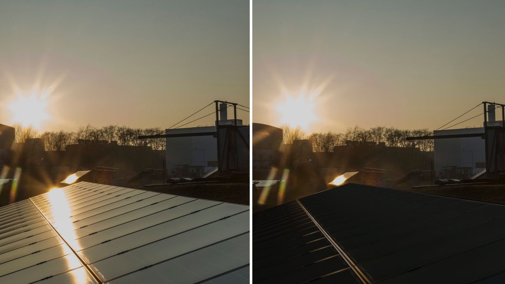
The high-tech company Phytonics, a spinoff from the Karlsruhe Institute of Technology (KIT), gets inspired by plants: The Phytonics film with micro- and nanostructures modeled on rose petals provides an anti-reflective coating for all kinds of surfaces, makes solar modules up to ten percent more efficient, and gives many objects a noble velvety appearance. At the Hannover Messe 2021 from April 12 to 16, the innovation will be showcased at KIT's virtual booth "Future Hub".
Press Release 029/2021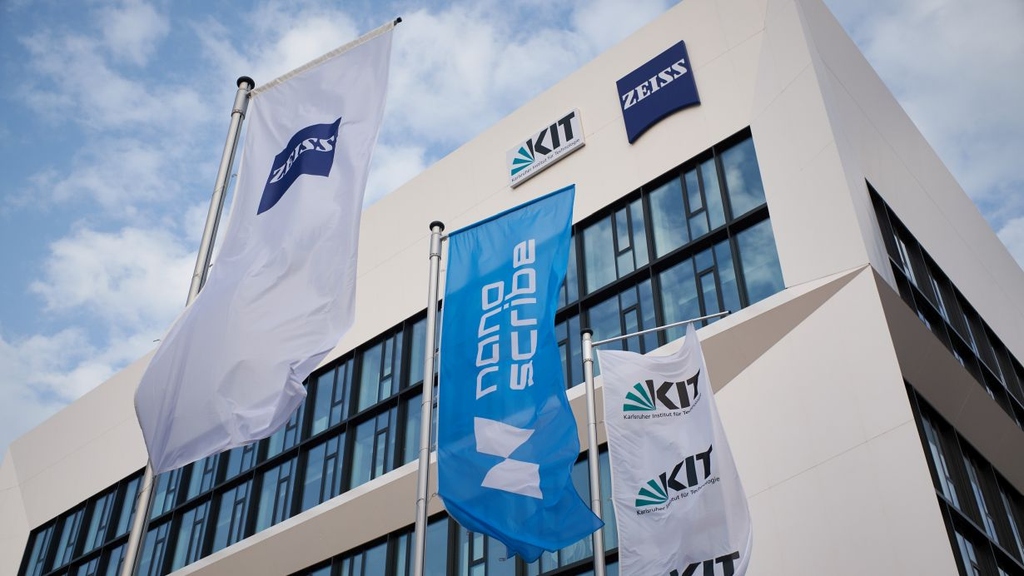
The ZEISS Innovation Hub @ KIT is a milestone in the longstanding partnership between ZEISS and the Karlsruhe Institute of Technology (KIT). In the new building on KIT’s North Campus ZEISS enables high-tech and digital startups to move into the Hub, and is driving its own innovation and new business activities. The Hub has seen a number of successful collaborations and projects since it opened in early 2020.
Press Release 005/2021